Pins & Signals
The ESP32-C5-WROOM-1U module's pins are split between board-managed functions (things the board itself wires up — buttons, I2C buses, alerts) and pins left free for your own use.
Pinout diagram
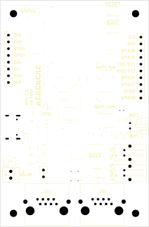
Draft, auto-generated from the PCB's own top-silkscreen text (tools/generate-docs-assets.sh)
rather than hand-drawn — every header pin's signal name is already printed on the physical
board, so this is what you'd see looking at the board itself. A polished, styled version may
replace this later.
For something more useful when you're actually holding the board: open the interactive
BOM — hover or click any reference designator to highlight
it on the board (and vice versa), search by part/value, and toggle top/bottom layers. Generated
by InteractiveHtmlBom from the same
.kicad_pcb source as everything else on this page.
GPIO map
| GPIO | Function | Category | Strapping pin? | Pull resistor | Notes |
|---|---|---|---|---|---|
| CHIP_PU/EN | Reboot button (SW1) | Fixed | No (dedicated EN pin) | R1 10kΩ pull-up to 3V3_SYS + C2 1µF | Reset button |
| GPIO0 | Boot/flash button (SW2) | Fixed | Yes — boot-mode select | Internal pull-up + R2 10kΩ external to 3V3_SYS | Hold during reset to enter download mode |
| GPIO1 | Unused | Free | No | — | Routed to expansion header J7 |
| GPIO2 | SDA_INT — LP_I2C_SDA | Assigned | No | R20 4.7kΩ pull-up to 3V3_SYS | Internal I2C data. Fixed-function LP pin; see below. |
| GPIO3 | SCL_INT — LP_I2C_SCL | Assigned | Yes — SDIO sampling/clock-edge select | R21 4.7kΩ pull-up to 3V3_SYS | Internal I2C clock. Fixed-function LP pin; see below. |
| GPIO4 | FG_ALERT (fuel gauge) | Assigned | No — deep-sleep wake capable | R401 10kΩ pull-up to 3V3_SYS | Fuel-gauge alert, wake-capable. Kept on its own net, separate from the charger's interrupt |
| GPIO5 | Unused | Free | No | — | Routed to expansion header J8 |
| GPIO6 | LED1_CTRL (status LED) | Assigned | No | — (push-pull output) | Drives LED1 through R3 (120Ω) |
| GPIO7 | Unused | Free | Yes — paired SDIO edge-select strap | — | Routed to expansion header J7 |
| GPIO8 | CHG_INT (charger interrupt) | Assigned | No | R24 10kΩ pull-up to 3V3_SYS | Short interrupt pulse; recoverable via I2C polling |
| GPIO9 | SDA_USER (user I2C data) | Assigned | No | R201 4.7kΩ pull-up to 3V3_USER | Feeds the I2C differential buffer + external STEMMA QT port |
| GPIO10 | SCL_USER (user I2C clock) | Assigned | No | R202 4.7kΩ pull-up to 3V3_USER | Paired with GPIO9 |
| GPIO11 | U0TXD | Fixed | No | — | Debug console UART, also routed to J8 |
| GPIO12 | U0RXD | Fixed | No | — | Debug console UART, also routed to J8 |
| USB_D− | USB_DN | Fixed | No | R7, 22Ω series | Native USB peripheral. The series resistor Espressif recommends. |
| USB_D+ | USB_DP | Fixed | No | R8, 22Ω series | Native USB peripheral. Shared with the charger's BC1.2 detection input via R9/R11, which ship as cuttable 0Ω bridges. See Notes. |
| GPIO15 | Reserved — in-package PSRAM chip-select | Reserved | No | — | Consumed inside the module, not by this board. See below. |
| GPIO16–22 | Not exposed | Reserved | — | — | Internal to the module, not broken out |
| GPIO23 | EN_3V3_USER | Assigned | No | R23 100kΩ pull-down to GND | Enables the switched 3V3_USER rail; defaults OFF at power-up |
| GPIO24 | Unused | Free | No | — | Routed to expansion header J8; free for reassignment |
| GPIO25 | Unused | Free | Yes — boot-mode strap, floating default | — | Routed to expansion header J8 |
| GPIO26 | Unused | Free | Yes — boot-mode strap, floating default | — | Routed to expansion header J8 |
| GPIO27 | Unused | Free | Yes — boot-mode strap | — | Routed to expansion header J8 |
| GPIO28 | Unused (biased) | Free | Yes — boot-mode strap, default internal pull-up | R4 10kΩ pull-up to 3V3_SYS | Routed to expansion header J8. R4 reinforces the strap's default state; C3 is an unpopulated 0603 tuning placeholder |
Why the internal bus is on GPIO2/GPIO3
The ESP32-C5 has one general-purpose I2C controller and one low-power controller (datasheet §4.2.1.3: "ESP32-C5 has an I2C and an LP I2C bus interface"). Two simultaneous I2C buses therefore need both.
The HP controller routes to any pin through the GPIO matrix, but LP_I2C does not — it is
hard-wired through the LP IO MUX to GPIO2 (LP_I2C_SDA) and GPIO3 (LP_I2C_SCL). So the
internal bus sits on exactly those two pins, and the user bus takes the HP controller on
GPIO9/GPIO10. Put the internal bus anywhere else and both buses contend for the single HP
controller, which won't build.
That pinning also buys something: the LP peripherals and LP CPU stay powered in deep sleep, so the charger and fuel gauge can be polled while the main CPU is off, rather than waking the whole chip to read a register.
Free IO
GPIO1, GPIO5, GPIO7, GPIO24, GPIO25, GPIO26, GPIO27, and GPIO28 are unused and available for
your own projects. All of them are routed out to the two expansion headers (J7 and J8),
which aren't fitted at the factory — solder a 2.54mm header strip to use them.
Note the strapping-pin caveats on GPIO7, GPIO25, GPIO26, GPIO27, and GPIO28 above: the MCU samples these at reset to select a boot mode, so check what each strap does before loading one down at boot. Exposing strapping pins on a header follows the precedent of Espressif's own DevKitC-1.
Special-function pins
CHIP_PU/EN, GPIO0, GPIO11–12 and the native USB pins are committed to fixed board functions — reset, boot select, debug UART and native USB respectively — and aren't available for reassignment.
GPIO15 is a module-level reservation, not a board one. This design uses the
ESP32-C5-WROOM-1U-N8R8 variant, where the R8 denotes 8 MB of PSRAM packaged inside the
module alongside the 8 MB of flash. That PSRAM's chip-select is wired to GPIO15 within the
module, so the pin never reaches the module's edge as a usable IO no matter what the host
board does. This board leaves it unconnected, and the firmware doesn't enable the PSRAM either
— so it is neither routed nor in use here. A module variant without in-package PSRAM would free
the pin, at the cost of the PSRAM.